
Synopsys announced availability of its first Multiphysics Fusion solutions for customer chip designs.
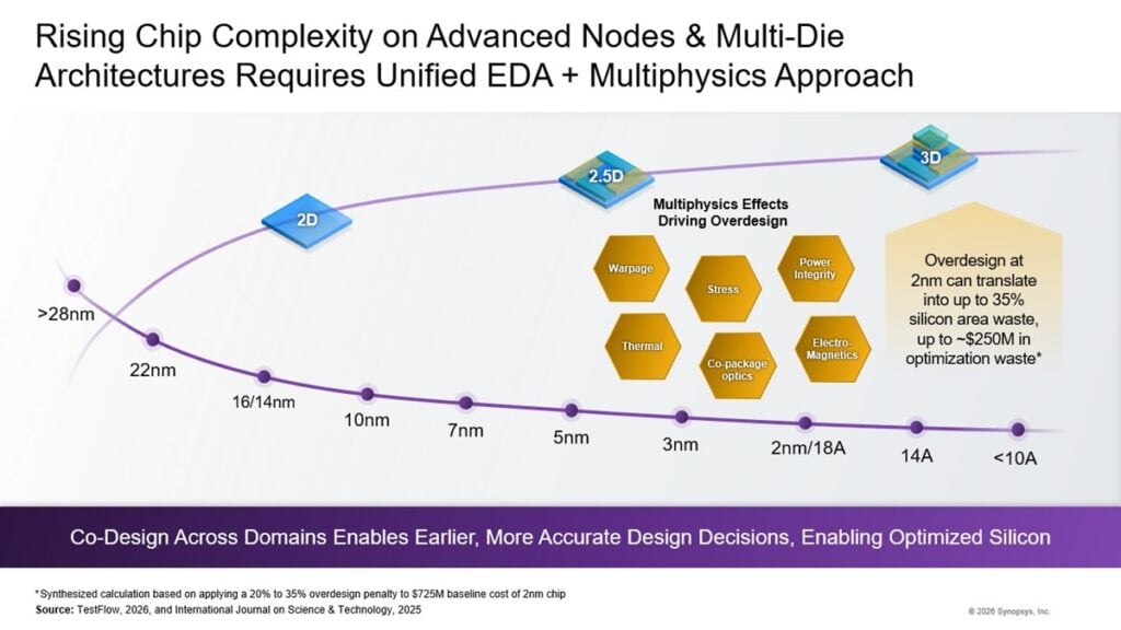
As chip complexity increases, physics-related challenges including signal integrity, power integrity, thermal integrity, electromagnetic effects, and co-packaged optics are becoming critical constraints.
That can hold back progress of electronic components, so Synopsys is working on solutions for advanced nodes and in multi-die architectures, requiring a unified electronic design automation (EDA) and multiphysics approach. The result is faster and less costly chips and systems.
The Multiphysics Fusion portfolio combines Synopsys’ AI-powered EDA solutions with Ansys golden signoff analysis across timing signoff, design closure, multi-die design, and analog workflows. Validated by market leaders, these solutions improve predictability and accelerate convergence for AI and high-performance computing systems.
I spoke with Hany Elhak, executive director of EDA Product Management at Synopsys, about this development. He is responsible for analog and mixed signal analysis at Synopsys and joint solutions developed at both Synopsys and Ansys, which merged with Synopsys in 2025 in a $35 billion deal.
Multiphysics is a concept that combines different kinds of physics, like the electrical physics that Synopsys knows well through the micro world of chip design, and the physics of systems that Ansys knew through its work with physics of the macro world, Elhak said.
“Multiphysics is fundamentally reshaping how advanced semiconductor designs are engineered, driving a shift from costly overdesign to integrated, system-aware co-design,” said Sanjay Bali, senior vice president of EDA product management and strategy at Synopsys, in a statement. “Our Multiphysics Fusion portfolio unifies Synopsys and Ansys technologies to embed physics directly into digital and analog workflows, enabling engineering teams to design across domains with fewer iterations, improved productivity and more optimized silicon for next-generation systems.”
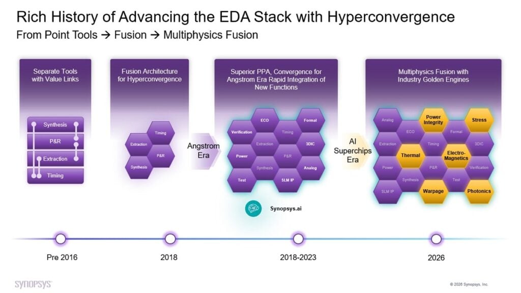
Fusion refers to the tighter integration between different tools in the design flow, he said. Elhak noted EDA tools used to be separated for different functions, with some value links between them. The tools were layered upon each other, from RTL down to the layout. Each step was separate. Now the tools have been brought together in a Fusion architecture, with tighter integration. Now, with multiphysics, the integration is combining the chips design tools with the system design tools and the analysis tools. It takes into account different physics like thermal, liquid, power, electrical and more, Elhak said.
“Now, chips are impacted by by other physical phenomena,” Elhak said. “For example, very large chips are designed at two nanometers and implemented inside a data center which will be impacted by thermal effects. So, thermal is another type of physics, just like electrical.”
One reason multiphysics is more important now is due to the complexities of chips today, where transistor sizes are shrinking and they are approaching physical limits. They can be impacted by heat, process variation, and voltage. The transistor is more susceptible to physical phenomena than other electrical properties. And it is no longer just one chip inside a package; it’s multiple chiplets, with each performing a certain function. A high-bandwidth memory package could be a stack of dies, or chips. Physics beyond electrical can influence this stack. And so engineers need to analyze all of these multiphysics effects, not just electrical effects.
“The chip design flows all come from Synopsys,” Elhak said. “All the multiphysics analysis is coming from Ansys. What we did in less than one year since the merger was completed is that we were able to make this fused or integrated technology, put it in the hand of the early adopters who have tested it and we have seen orders of magnitude of improvements on their design force.”
Enabling Multiphysics-Aware Co-Design Across the Chip Design Flow
Building on the vision introduced at Synopsys Converge 2026, the first Multiphysics Fusion solutions include targeted GPU-accelerated flows powered by Nvidia CUDA-X libraries such as cuDSS:
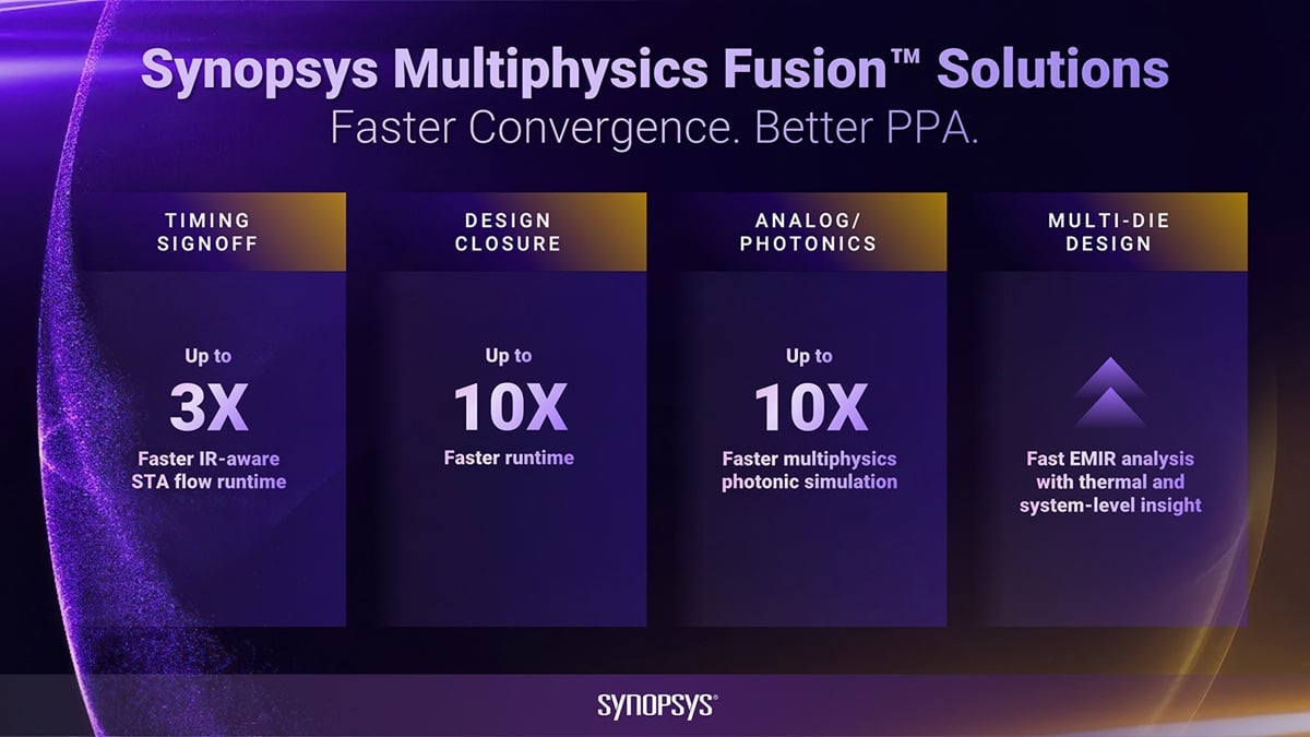
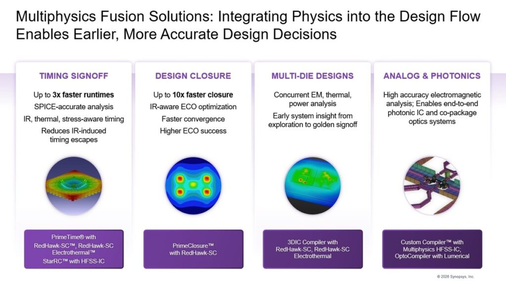
- Multiphysics Fusion for Timing Signoff: Enables up to 3x faster runtimes, SPICE-accurate
multiphysics timing analysis. Integrates Synopsys PrimeTime with RedHawk-SC and
RedHawk-SC Electrothermal, along with unified full-spectrum RC extraction using Synopsys StarRC and multiphysics HFSS-IC, to incorporate IR, thermal, and stress effects, improving margins and reducing IR-induced timing escapes. - Multiphysics Fusion for Design Closure: Delivers up to 10 times faster design closure with higher engineering change order (ECO) success rates and improved power, performance and area (PPA). Combines Synopsys PrimeClosure with RedHawk-SC to embed power integrity into golden signoff optimization, accelerating convergence with fewer iterations.
- Multiphysics Fusion for Multi-die Designs: Unified Synopsys 3DIC Compiler platform with
RedHawk-SC, RedHawk-SC Electrothermal and multiphysics HFSS-IC for concurrent power integrity, thermal, and electromagnetic analysis, providing early system insights from exploration to golden signoff with correct-by-construction design. - Multiphysics Fusion for Analog & Photonic Design: Integrates Synopsys Custom Compiler
with multiphysics HFSS-IC for on-chip, high accuracy electromagnetic analysis into the
analog design flow, and Synopsys OptoCompiler with Lumerical enabling end-to-end
photonic IC and co-packaged optics systems.
There’s a way to explain what this means in the real world. I have to make sure there is enough airflow for my gaming PC so it doesn’t overhead. I make sure it’s far from walls and the door is open in the room so it gets good air flow. That’s a design consideration on the system level, where Ansys operates. But on the chip level, the same physics related to heat applies.
When you design a chip, you have to make sure any given transistors are far enough apart from each other so that they don’t overheat each other, or that a metal layer is thick enough so it can carry heat out of the system adequately, Elhak said. The combination of the physics of the system and the chip is multiphysics engineering.
“You’re describing it now at the system scale, but at the transistor scale it is the same physics related to heat,” Elhak said.
Demonstrating Real-World Impact with Market Leaders
Companies like Mediatek, Samsung, Cisco and Nvidia have tested these tools.
Early engagements with leading semiconductor and systems companies validate the value of
Multiphysics Fusion solutions.
“As multi-die integration becomes increasingly important for high performance compute platforms, it’s critical we make the right system-level design decisions early in the development process,” said Harrison Hsieh, vice president at MediaTek, in a statement. “By unifying multiphysics analysis and timing signoff across digital, analog, photonic and multi-die designs, Synopsys Multiphysics Fusion technology gives us earlier insight into cross-domain interactions across silicon, advanced packaging and optical domains, which makes it possible for us to improve predictability, reduce late-stage rework, and achieve a runtime that’s 10 times faster than before.”
“Advanced AI and high-performance computing platforms are pushing chip design beyond traditional workflows, and to deliver greater performance, efficiency and reliability at scale, multiphysics-aware co-design is essential,” said Tim Costa, vice president and general manager of computational engineering at Nvidia, in a statement. “Synopsys is using Nvidia accelerated computing and CUDA-X libraries, including cuDSS, which delivers up to 13x GPU acceleration, to scale increasingly complex SPICE simulations, electromagnetics, and power-integrity workloads. In addition, Synopsys Multiphysics Fusion solutions enable up to five times faster design closure and up to 86% IR fix rates in selected pilot designs.”
IR, or voltage drop, relates to power integrity. If it drops so low that it can’t cause a transistor to switch, that’s classified as an IR violation. Normally, Ansys could catch this kind of problem. Now it is bringing this kind of analysis inside the chip as well.
“By finding these errors through the design closure tools and automatically fixing it, we are avoiding weeks of time wasted in the design cycle,” Elhak said.
Since the merger closed, Synopsys has put these tools in the hands of major customers.
“Accurate timing signoff at advanced nodes requires a unified approach that accounts for IR drop, thermal, and stress effects directly within timing analysis,” said Hyung-Ock Kim, vice president and head of the Foundry Design Technology Team at Samsung Electronics, in a statement. “Synopsys’ Multiphysics Fusion technology provides a unified, all-aware timing signoff platform by integrating PrimeTime with multiphysics insight, delivering SPICE-accurate correlation and enabling margin recovery. This is increasingly important as we pursue higher levels of integration, performance, and reliability across advanced process and multi-die technologies.”
In addition, the Cisco Silicon One group is leveraging Synopsys Multiphysics Fusion technology to unify IR drop effects within signoff design closure to gain earlier, more accurate visibility into real-world conditions. Combined with signoff-accurate, timing-aware IR fixing, this enables predictive optimization—helping Cisco Silicon One converge on power integrity issues faster, deliver better PPA, and achieve significantly faster runtime.
Availability
Multiphysics Fusion solutions for timing signoff, design closure, multi-die design, and analog and photonic design are available today.
In summary, now you know why the $35 billion merger between Synopsys and Ansys happened.
Elhak gave a nod when I said this. He added, “This is the first wave, but more is coming.”