
Synopsys is building an open, secure, hardware accelerated agentic AI stack in collaboration with Nvidia to cater to use cases from silicon to systems.
Applied Materials is also collaborating with Synopsys to accelerate complex quantum chemistry simulations for large-scale dynamic materials modeling by up to 30 times using Synopsys QuantumATK optimized with Nvidia.
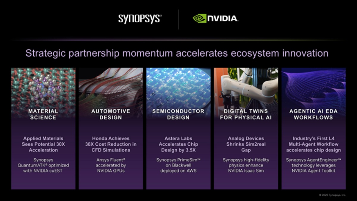
Synopsys at Nvidia GTC 2026 is showcasing the progress and impact of its strategic partnership with Nvidia to revolutionize design and engineering across industries. R&D teams, from the semiconductor industry to aerospace, automotive, industrial and beyond, face significant engineering challenges including increasing workflow complexity, escalating development costs, and time-to-market pressure.
At GTC, Synopsys is demonstrating how integrating the strengths of NVIDIA’s AI and
accelerated computing with Synopsys’ market-leading engineering solutions is enabling R&D teams to design, simulate, and verify intelligent products at lower cost with greater precision and speed.
“Traditional engineering methods can no longer keep pace with the complexity of today’s software-defined, intelligent systems,” said Sassine Ghazi, CEO of Synopsys, in a statement. “Together with ecosystem partners, Synopsys and NVIDIA are re-engineering how products are designed and developed. By enabling the co-design of electronics and multiphysics, accelerating compute-intensive workloads and applying the power of digital twin for virtual prototyping, we are helping customers engineer the future.”
“AI and accelerated computing are fundamentally reinventing engineering — from how products are designed to how they are built and operated,” said Jensen Huang, CEO of Nvidia. “Modern engineering happens inside simulations and digital twins. Together with Synopsys, we are combining Nvidia CUDA-X, Omniverse, and AI with Synopsys’ silicon-to-systems platforms to reimagine engineering for the age of AI and turn growing complexity into a powerful advantage.”
Synopsys has the industry’s broadest portfolio of engineering applications that enable AI and GPU-accelerated computing across engineering workloads — making engineering smarter, faster, and more intuitive. Customers are utilizing Nvidia GPU-accelerated applications from Synopsys to speed up compute-intensive workloads.
Today, Synopsys announced several examples:
Applied Materials is collaborating with Synopsys and Nvidia to advance AI and quantum chemistry R&D with accelerated materials modeling. Leveraging Synopsys QuantumATK’s new integration with Nvidia cuEST, early results from Applied Materials show a potential 30X speedup for complex quantum chemistry workloads compared to open-source models running on CPUs. Previously, Applied Materials achieved an 8X simulation speedup leveraging NVIDIA GPUs compared to multi-core CPUs for multi-nanometer amorphous systems featuring approximately 25,000 atoms.
“Applied Materials is working with Synopsys and Nvidia to accelerate materials engineering innovations that can deliver tremendous improvements in energy-efficient performance of advanced semiconductor devices,” said Gary Dickerson, CEO of Applied Materials, in a statement. “This collaboration allows us to significantly reduce the time it takes to run simulations of material behavior at the atomic level, thereby enabling the industry to bring chip design breakthroughs to market faster.”
Honda has also realized unsteady, large‐scale, high‐fidelity CFD that was previously impractical on CPUs through GPU acceleration on Ansys Fluent® fluid simulation software.
“We achieved 34x faster computation and 38x cost reduction using four GB200 GPUs compared to 1,920 cloud-based CPU cores,” said Yusuke Uda, Assistant Chief Engineer at Honda, in a statement. “Through close collaboration with Synopsys, Honda is accelerating the migration of its CFD simulations from CPUs to GPUs. This advancement enables us to continue delivering safer, higher‐quality products to our customers at appropriate cost, with consideration for the environment.”
As AI scaling drives the need for high-speed connectivity to move massive datasets with near-zero latency, advanced chips with ultra-high-speed SerDes interfaces require extensive circuit-level simulations.
Astera Labs achieved a 3.5X speedup running Synopsys PrimeSimTM using B200 GPU accelerated EC2 instances on AWS compared to CPU-only instances, dramatically shortening design validation cycles and enabling faster time-to-market for next-generation connectivity solutions.
The seamless access to GPU resources on AWS enables Astera Labs’ design teams to focus on innovation rather than infrastructure setup, further accelerating time-to-market while supporting superior design accuracy.
“The collaboration between Astera Labs, Synopsys, Nvidia, and AWS is transforming our ability to design advanced blocks for AI connectivity silicon,” said Jitendra Mohan, Chief Executive Officer of Astera Labs, in a statement. “By harnessing the power of Nvidia B200 GPU-accelerated computing on AWS, we have significantly reduced simulation times and enhanced design accuracy, allowing us to deliver innovative connectivity solutions to the
market faster than ever before.”
“Astera Labs’ work with AWS — achieving dramatically faster design cycles for the connectivity solutions that power AI — demonstrates how cloud technology is transforming innovation across entire industries,” said Ozgur Tohumcu, General Manager of Automotive and Manufacturing at AWS, in a statement. “We’re enabling companies to access the most advanced computing tools instantly, changing how breakthrough technologies get built without the burden of managing complex infrastructure.”
Skip to main content
Ask or search
CtrlK
Share
synopsys multiphysics
More options
Dean Takahashi
Today at 5:06 pm
31 min
copy summary
Summary
Transcript
Edit Transcript
Keywords
Ansys, Synopsis, digital twins, multiphysics analysis, chip design, power integrity, electromagnetic tools, thermal effects, design closure, timing sign-off, analog circuits, photonics, AI accelerators, autonomous vehicles, multiphysics fusion.
Speakers
Speaker 1 (85%), Dean (12%), Speaker 2 (3%), Speaker 3 (<1%)
Is our executive director on the EDA product management team. He oversees the portfolio that you’re going to learn more about. Dean knows as well. Hani definitely follows Ansys for a long time, and very much tuned into digital twins and video collaborations, and then everything advanced semiconductor related. So pleased to introduce you, Dean. I don’t think you’ve met Hannie before, but I will. I sent, so I sent Dean the announcement, and Dean, I’ll follow up with the final. We have it now, and a couple images from this presentation that you can reference as well, if it’s of interest. If you find that you do want to write,
okay? Yeah, is this.. is this also coming from the aunts on the side of the house or versus synopsis.
Yeah, I’ll let.. well, it is about.. we think of it as one house now, but that’s a great segue. I’ll turn it over to you and honey to dig into it, and I’ll drive from my side.
Okay,
all right. So, Dean, why don’t you tell me about the different things you are covering on Ances before, so I can go to,
I think, you know, things like the big merger, I think a lot of things that say come out of talking about digital twins and simulation, and some crossover with the things on the consumer side, like games, as well. Your CTO, I forget his name, but we talked about sort of the evolution of, I think, digital twins, and then, yeah, I’ve covered chips for some decades, I guess, right. And so I happen to cover mostly the crossover, mostly games, but I still keep a foot in technology in general and chips in particular as well, so
this is perfect, because basically what we are announcing now is the integration of the multiphysics analysis from Ansys with our chip design tools, so basically bringing in all the different analysis or the different analysis from answers, such as power integrity tools like Redhawk, and I’m sure you’ve covered Red Hawk and Red Hawk SC, and these before, our like electromagnetic tools like HFSS and electro thermal tools into chip design flows from design closure to sign off to analog and photonics,
and I guess, how did you yourself get into this? I guess what sort of branch of the technology did you move into first year
as myself as Hannah or at Synopsis or
you, yeah,
all right, so my background, I am I’m responsible for the analog mix signal line of business here at Synopsis and even before the Ancestors integration of Ancestors joined through the merger, even before the merger, I was involved in all the planning for the merger, and and after that I’m, I’m responsible for the joint solutions, which is all the technology integration between assets and synopsis, not just in the analog mix signal, which is my background, but across the board. So I was from the product management group, I was in charge of of the develop of the definition development and testing of these products with customers, so that’s how I’m personally involved in that project. So, I’ve been working all the ancestors folks, I’m sure you have worked with pretty Gupta and Steve Feitel and Jim Delap, and this team I was,
and what
is faith between them and their counterparts at synopsis, and to build these joint solutions to that, and how do we just sort of convey this concept of multiphysics fusion to regular folks, like, what, what does it mean? I guess what we mean by multiphysics fusion. So, fusion, if we go to the next slide, please. Kelly, fusion is the term we use at synopsis for. The tighter integration between different tools in the design flow, so if we look at the left-hand side, this is what this is. How EDA flows used to be separate tools with some value links between them. Then we took it to the Fusion technology, where we brought in technology, for example, like synthesis and latent route, so more designers would do, would start with RTL description, hardware description languages, do synthesis, get to the gates, take the gates, and start doing place and route to get to the layout. Each step was separate. We brought these different steps together in a flow where you’re starting from the RTL, from the hardest hardware description all the way to the GDS to the layout that you sent to the foundry. So this tighter integration between the tools is what we call the fusion architecture. Now we are taking, and we kept expanding this fusion architecture, started with simple and trace and route, then it included extraction, timing, power, and now what we are doing is we are taking this fusion architecture we are integrating into a dean’s tool, so bringing the ability to analyze our integrity and I analyze thermal electromagnetic stress inside every step in the chip design tool, and that’s what we call by fusion. It’s bringing this analysis into the tool, so it’s not like two tools talking to each other through some kind of a standard file. It is the analysis integrated into the implementation or sign off tool, so the results that you get from, let’s say, if you’re doing timing analysis with a sign of tool, your timing analysis becomes thermal aware, becomes power integrity aware. It’s not like I’m running thermal analysis, running power integrity, saving results into a file, and then reading it when I’m doing timing, and that’s basically what we mean by theory,
and multi physics itself, I don’t quite get that concept, is it meaning blending together different sort of, I don’t know, levels of detail in chips and design that have to do with physics, or
that’s that’s an interesting question, because I would say maybe multi physics is our our synopsis view of the rest of the world, as we work on chip design, we deal with one type of physics, which is the electrical. We deal with current, voltage, and power, right. That’s let’s think of it as this is the electrical domain, one type of one domain of physics, and that’s where chip design was in for its entire history. Now, chips are impacted by by other physical phenomena, for example, chips in, you know, very large chips designed at two nanometer or 14 angstrom, and implemented inside a data center will be impacted by thermal effects. So, thermal is another type of physics. So, just like electrical, you have voltage and current, thermal, you have temperature and heat flow. So, it’s a different type of physical analysis, and the same with mechanical, the same with power integrity, electromagnetic. Now we are talking about electromagnetic waves and electric fields and magnetic fields, and so what we mean by multiphysics from our chip design perspective is that we are moving from one physics, which is the electrical domain, to multi physics, which is electrical, thermal, mechanical, optical, and electromagnetic.
Okay, you can go ahead, it’s your slides in front.
Okay, so, so, yeah, so, so, why the question is, why multiphysics is important now, as we are moving, as chips are moving, you know, there are two, two directions for the complexities of the chip today, one that. Direction is the shrinking of the size of transistors, and shrinking the size of transistors brings the transistors more towards the physical limit, so you are, you are impacted by, you are impacted by heat, you are impacted by process variation, you are impacted by every transistor is receiving power through a power delivery network, a PDN. The properties of the transistor is impacted by very slight changes in that PDN. So, as we are shrinking the size of the transistor from five to three to two to 14 angstrom to below, the transistor is more susceptible to physical phenomena other than the electrical properties, and the second, and the second dimension is those chips, are you know, it’s no longer one chip inside the package, it is multiple chiplets, each one performing a certain function, that are constructed on an intercourse in on a substrate, and and integrated into the package. So now it’s going to, like, if you look at memory, for example, memory was basically a memory die inside the package. Now you look at high bandwidth memory, HPN. It’s a stack of dies. You have a base die with all the communication and the digital functions, and then on top of it is stacks and stacks and stacks of chips used for memory, and each one of them is heating the other one, each one of them, when it heats, it expands, and it causes mechanical stress that impacts itself on the other one, so the second dimension really is the integration of these different chips in a structure inside the package, so in one hand transistors are getting smaller and their numbers are getting bigger inside the one chip and on the other hand this one chip is integrated with lots of other chips in the same package and that makes at the different levels of the chip let of the chiplet and the transistor and at the that system level that includes multiple chips and inside the package you need to analyze things like thermal stress, power integrity, electromagnetic mechanical warpage, and that’s why there is a need to analyze all these multiphysics effects in the context of the electrical analysis that we normally do to design these things,
interesting, I guess it seems like maybe a bunch of that physics must have come from Ansys on the one hand, whereas a bunch of the chip physics must have come from synopsis.
Exactly, the chip design flows all come from synopsis. All the multiphysics analysis is coming from Ansys, and what we did in less than one year since the mercury was completed is that we are able to make this fused or integrated technology in the hand of the early adopters who have tested it and have seen orders of magnitude of improvements on their design force.
Okay, as we will see in next slide. Interesting.
So, so what we are really announcing now is that we are integrating these different multiphysics analysis in different stages of the chip design flow, one of them is timing sign off, so timing sign off is about making sure that the delays resulting in from the switching of the different transistors on the chip is is is within the clock frequency, so it’s not impacting the performance of the chip, so when you say I have this 32 gigahertz PCIe chip, or I have like a three gigahertz microprocessor, or this, there are functions that need to be performed within this picosecond of time, and, and this, and this, this timing sign off is impacted by all the different physical phenomena, like, like thermal and power integ. It and stress and in in the traditional flows today I see designers are running these different analysis separately generating reports and then using these reports to to add margin to the design so if I say, “Oh, my delay is one picosecond. Oh, but it could be more, it could be less, because of variation in thermal effects, because variations in the power supply. What designers do, they add margins, and when they add these margins, these margins will either make their chips lower or to keep the performance they need to use bigger transistors to use buffers and that will make the chip bigger and they will waste area or they can keep their area and and keep their performance and consume more power to get the same results, so you’re either losing on power, on performance, or on area because of these margins, and this is over design now. By making this information available to the to the team, to the design team at the time of their timing sign off, they know exactly what is the effect of thermal? What is the effect of stress? What is the effect of power integrity? Because now they can get the timing information, how the timing information is impacted by these different physics, and by doing that, they, they don’t need to put the margins anymore, and they can make their design smaller, faster, and consume less power.
Interesting,
and the same applies to things like design closure, applies to analog, applies to photonics, and applies to the design of d IC, and these chips are used in many applications. They’re used in the AI accelerator, in high-performance compute systems, in in physical AI, in robotics, in autonomous vehicles. It’s, it’s these chips are everywhere, and and we are using it in several, we are using multi physics in different use cases, like understanding how timing of the circuit is impacted by these physics, how how the how violations that happen due to problems, say, with the power supply or thermal issues, can be detected and fixed without having to reiterate the design multiple times, and the same to at the chip level and also at multi-disciplinary always
have to make sure my gaming PC is separated from the walls enough and has the door open, so it gets a lot of airflow. These sound like things that affect the chip in some way, right?
Actually, it does. Yeah, it is exactly, you know, it’s the same physical phenomena applied at different scales, you know. It’s you’re describing it now at the system scale, but at the transistor scale it is the same, you know, you want to make sure these two transistors are far enough apart from each other so that not one of them heats the other one, and you want to make sure that they are connected with a wide enough metal so that this heat gets dissipated. It’s exactly the same phenomena you are describing at the macro level is repeated at this nano and angstrom level.
Interesting, yeah, it’s the same physics, different scale. Yeah, that’s a good way to explain it, I think. Yeah,
so, so the first, yeah, the first one of the first I would say EDA flows where we integrated these multiphysics is in design closure, and design closure is about detecting why we, why we are signing off the chip, we are detecting certain errors or violations, and trying to avoid them by making what we call ECOs, engineering change orders, so we bring it back to the design team and say fix this and change it, you like, if let’s say, if, for example, a. A timing I have, like, oh, there is this path in my chip that is has a delay longer than the clock, and it’s
sorry, in this graph, what does IR stand for? Is that infrared, or is it something else?
Oh, IR here stands for I is for current and R for resistor, so as in ohms low V equal I R, so here I R drop is voltage drop. So basically, what we are talking about here is the power integrity. So think about it like every transistor is connected to the power supply,
but
it is not connected to the power supply within, like with an ideal wire. It’s connected to the power supply through a very complex power delivery network. The power delivery network takes power from the supply into through the PCB into every package and inside every package through the interposer to every chiplet, and then inside every chiplet there is a power delivery network that will take the power all the way to every individual transistor, so this all these, the traces on the PCB, the connectors on the package, the traces on the interposer, and the metal layers inside the package, they all contribute to resistance that will cause voltage drop as the signal goes from the power supply to the to the transistor, and every transistor gets that signal through a different journey, so every transistor gets a different version of this power, either a little bit higher, a little bit lower, and it changes, sometimes it’s too low, so it’s not enough to cause the transistor to switch, and that’s what we would call this as an IR violation. My power delivery network consumed all my current, nothing arrived to my transistor, or very little arrive to my transistor to make it switch, or sometimes it switched, but it switched too slowly, because the current is not big enough, or the voltage on it is not high enough, so all these phenomena are what we refer to as power integrity, or IR analysis, and this is one of the multiphysics analysis, one of the very, I would say popular multiphysics analysis from ANSYS, where the Red Hawk family is, is, is famous for, and we are bringing this analysis now inside the EDA tool, so you can detect these IR violations and an autofix it without having to go for these four to six weeks of iteration, where, oh, I have an error, I need to have an engineering change order. Please fix those transistors, redraw the power delivery network for me, on you know, on the chip, and then they change it, and that this is like weeks are wasted whenever these errors are discovered, and by finding these errors through the design closure tools and automatically fixing it, we are avoiding weeks of time wasted in the design cycle.
Very good,
and the other area where we are integrating the multiphysics tools in timing sign off, and this is in making sure that every path in my design, the delay in that path is according to the specification and can be performed in the time required by the spec of the clock and and and this this timing also is impacted by thermal effect by IR drop from the power delivery network by stress and now instead of running all these analysis separately, and then adding margins to the design to account for timing, we are doing that directly inside the timing tool, so this way we get better accuracy, and we reduce the pessimism that adds to that the pessimism that requires sorry to that the pessimism that requires the additional thank you and just like the we are integrating the. Different analysis at the chip level, we are integrating it also at the multi chip at the multi dye level. So, as we are integrating these different dyes together, they are connected through interposers, where I need to analyze the, you know, I have long signals that are impacted by electromagnetics, so I need a tool like HFS, for example, from Ansys to analyze the electromagnetic effects. I need to analyze the thermal effects with a tool like Icepack from Ansys, because now all these chips are packed together inside one package, each one of them heats up and heats the other ones. So now we are bringing all these different analysis into the multi dye design flow, and then lastly is analog anthroponics, so analog circuits, and if you think of all the chips that you know we always think of chips as microprocessors and GPUs, but in, you know, all these interestingly, like, you will not be able to use a CPU or a GPU unless you’re typing on the keyboard or looking through the monitor, and if it’s in a physical AI system, there is a motor that needs to be operated, and there is a sensor that detects motion, or detects light, or detects, so all these are done by analog circuits, and analog circuits today, in the world of physical AI, and in the world of autonomous vehicles, are as important as if not more important than the brains or the the micro, the microprocessors and the GPUs, and and we are, and these these analog circuits now operate at very high frequencies, and that requires electromagnetic analysis and requires, you know, there is, as the frequencies even get higher, you cannot just transmit the signal through copper, you need photonics, and today full packages, optics is one of the technologies that are that is going to be widely used in data centers, it’s like, instead of, we are not just connecting servers with each other with with optical fibers, we are actually connecting the chips with each other, and inside the dyes inside the chips with photonics, and we are, we are using the, we are integrating the I would say the golden photonic simulators like numerical from Ansys with our optical and analog design tools.
So we are integrating HFSS for electromagnetics, we are integrating numerical for optical inside our analog design platform to allow for all these different effects in real time across the design time, comic orders of magnitude in performance, as you can see, and these technologies, it’s not just we have been building the technology, but since the merger was closed, we have been working with customers in understanding their needs, in working on their on their high value problems, and and all these customers, like Media Tech, Nvidia, Samsung, they all have tested these tools and and reported the results that you have seen in the previous slides, so So, yeah, so in closing, this is the first wave of our multiphysics fusion solutions, and by multiphysics fusion means we are bringing the different physical analysis tools from ANSYS and integrating it into the design tools from synopsis across the across the overall design cycle from from design to implementation to sign off and from chip, whether it’s a digital chip, analog chip to the multi dye and the package in order to give designers accurate information about the different physical phenomena as they are designing the chips, so that they can, as they can measure, measure all these different physical phenomena, they don’t have to estimate it. Or account for it by adding margins over designing and, and losing either losing area, losing power, or losing performance, losing performance, so it is as you have seen, there is order of magnitude of improvements that are offered through the integration of these different tools across the overall design,
nice. Now I guess we’ll get a better idea of why this $35 billion merger happened.
I would say yes, this is the first wave, but more is coming.
Okay. All right. Very good. Thank you very much,
Dean. Appreciate your time. I’ll follow up with the final release in just a minute, and a couple visuals from the presentation that Honey took you through. Let us know if you have any questions as you digest it, and we appreciate connecting with you today.
All right, awesome. Thank you. All
right. Talk to you soon. Thank you. Thank you, honey. Bye bye.
How accurate was this transcription?
00:0031:18
1x
All transcriptions completed