
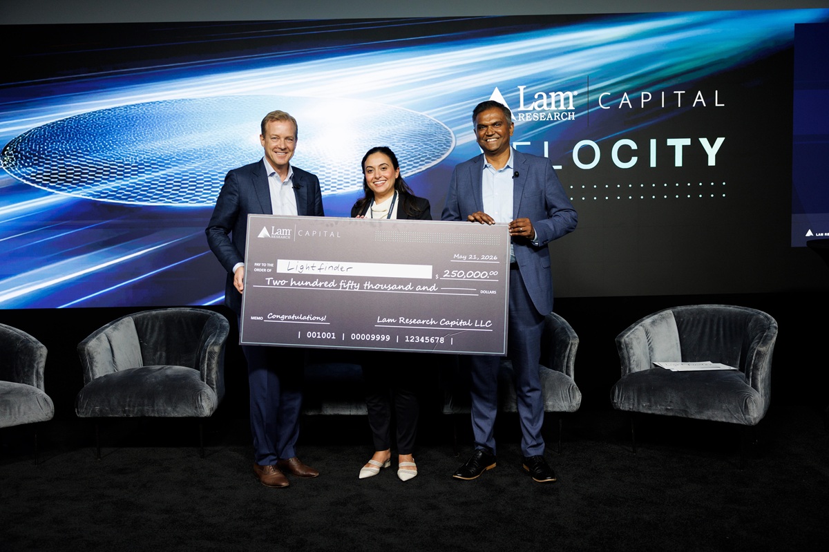
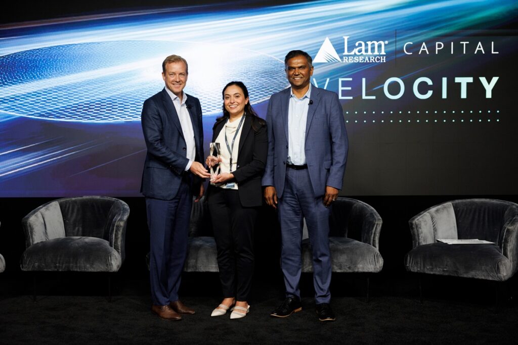
Lam Research awarded its $250,000 investment offer to Lightfinder at the end of its recent venture competition at its Silicon Valley headquarters.
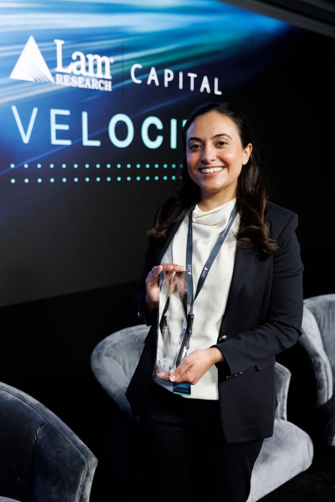
The winner was Lightfinder, which is making chip-scale optical instruments for sensing. Lighterfinder CEO Diana Mojahed was there to accept the award. The event was part of Lam Research’s fourth Lam Capital Venture Competition at Lam’s Silicon Valley headquarters in Fremont, California.
Lightfinder beat out 10 finalists from a total of 180+ international applicants who competed in live pitch competition for the prize. Lam Capital, the corporate venture division of chip equipment maker Lam Research, holds this biennial event to surface talented startups that can feed the semiconductor ecosystem. The chip equipment industry is vital since large chip factories now require investments of $20 billion to $65 billion, and much of the investment comes in the form of equipment inside the factories.
When she won, Mojahed said, “I was shocked” in a good way.
Now the company will be able to hire people and do more validation work on the tech in a more expedited way.
“We were very pleased with first the turnout, the interest, the quality of the the startups, the more global representation of companies that presented and outstanding conversations with investors,” Kevin Chen, managing director at Lam Capital, said about the event in an interview with GamesBeat.
To date, Lam has awarded $1 million to startups since the 2019 start of the events.
“To my knowledge, this is the only such event in our industry that has prize money
attached to it for the semiconductor industry,” Chen at Lam Capital. “That long-term commitment that we’ve been doing this every other year for the last seven years has resulted in it becoming a place where these conversations can happen, and I think that’s a big reason why we had our biggest turnout.”
The companies invited represented different parts of the AI backbone: advanced manufacturing, metrology, advanced packaging, robotics, and more.
Lightfinder’s mission
Lightfinder develops chip-scale spectrometers and imaging systems that deliver lab-grade optical sensing in a miniaturized, scalable form. Built on silicon photonics and paired with intelligent software, the platform enables real-time, in-situ analysis in places legacy instruments can’t reach—from inside semiconductor process tools to the factory floor—powering critical decisions in advanced manufacturing, telecommunications, and beyond.
Lightfinder’s tech could make it easier to do inspection for semiconductor chips, but Mojahed said chips are only one potential market for the technology. To date, the company has raised just under $500,000 she said.
Underneath the surface of a device, Lightfinder will be able to find defects and it can do it non-destructively, Chen said.
“It can analyze sub-surface features using silicon photonics,” Chen said.
Mojahed said the AI-powered tech leverages silicon photonics to miniaturize complex bulk optical instruments into a miniature chip-based system that serves as the hardware, and then it paired with AI algorithms that can interpret the measurement signals.
It’s like a traditional spectroscopy instrument, but miniaturized so that it uses near-infrared sensing to detect structures within solid objects or liquid. I’ve seen companies like Consumer Physics and Agate Sensors try to do this with materials sensing on smartphones.
Mojahed worked on this for eight years through her PhD and post-doctoral work before spinning it out of MIT in November 2024. The startup has three people now.
“My career so far has been all about optical instruments, and once I realized the power of silicon photonics to take what we were doing in optics, miniaturize it, maintain the performance, and in some ways exceed the performance, I devoted my whole career really to doing that,” Mojahed said.
And during that time, the datacom market really pushed what silicon photonics could do at scale, and Mojahed said, “It was a great time to ride on that.”
MIT helped the deep tech entrepreneurs figure out how to turn the tech into a startup that could commercialize the tools for multiple applications.
Mojahed said she believed the judges voted for her company because they appreciated the novelty of the technology and the potential it has for bringing high performance sensing into a small form factor, coupled with the fact that there are so many opportunities.
“We’re addressing the points that have made it not possible until now,” Mojahed said.
Mojahed said the tech could be useful across the spectrum of equipment that manufactures all sorts of chips. An rather than just monitor patterns in chipmaking that are captured at a point in time, the spectroscopy in this case could be used to measure the materials going through a factor in real time. The tech might become a hardware-based module within a piece of chipmaking equipment.
There’s an analogy here. It’s like how Apple Watch and health apps brought health sensing out of hospitals — where you might get test once in a while — and onto your wrist where the sensing could happen in real time.
“We’re doing something like that, but for industrial customers,” Mojahed said.
And in that case, the tech used for chip inspection has to be much more accurate than something like a watch.
“We achieve an optical instrument quality now that is not on your wrist but it’s a small scale sensor that can fit in many places and unlock new insights that you couldn’t do before because you’ve always used large heavy equipment where you have to sit and push buttons on,” Mojahed said.
Mojahed reiterated that this isn’t just limited to semiconductors and there are other markets for it.
The Lam Capital Venture Competition
Participating startups were at the leading-edge of advanced robotics, generative and physical AI, heterogenous integration, semiconductor manufacturing, photonics and other disruptive technologies that may build the future of the “AI Backbone.”
Leaders from Intel Capital, Nvidia, AMD, TMSC, BlackRock and other leaders about the trends and challenges in capital investment and semiconductor technology. Lam’s COO Sesha Varadarajan and Audrey Charles, president of Lam Capital, hosted the event.
Past finalists have become Lam Capital portfolio companies, led multi-million-dollar investment rounds and had partnerships with Fortune 500 companies. Lightfinder will join Lam’s family of 40 portfolio companies.
The AI era is pushing the semiconductor industry to innovate, scale and collaborate with faster velocity than ever in its history. The Lam Capital Venture Competition underscores Lam Research’s focus on fostering innovation and building a robust semiconductor ecosystem, said Chen.
Previous finalists have become Lam Capital portfolio companies, had partnerships with Fortune 500 technology leaders and led multi-million-dollar funding rounds.
4th Lam Capital Venture Competition Finalists: Selected from over 180 applicants, the finalists came from Silicon Valley, South Korea, Taiwan and beyond. They included:
- Flexify.ai (San Francisco Bay Area, U.S.): Industrial AI agents for equipment design and procurement
- Trener Robotics (San Jose, U.S.): Formerly T-ROBOTICS, a Physical AI company delivering skills models for rapid robot training and deployment
- Lightfinder (Massachusetts, U.S.): Chip-scale optical spectrometers
- Fringe Metrology (Arizona., U.S.): Structured light-based surface metrology for wafer shape and surface characterization
- NSC (Singapore): Heterogeneous integration of III-Vs to CMOS for photonic devices
- SemiAI (South Korea): Virtual metrology software for semi manufacturing
- TDS Innovation, Inc. (South Korea): Lateral growth process and tools for 2D materials deposition in semiconductor manufacturing
- Vertical Compute (Belgium): 3D magnetic vertical integrated memory
- Amazing Cool Corporation (Taiwan): Graphene-infused copper composite material to enable high-performance semiconductor systems
- Meukron Technologies (India): Provider of electrochemical etch fabrication technology for through-glass via formation
There were discussions on the challenges in advanced packaging and training robots based on physical AI systems. Meukron from India is figuring out how to drill holes in glass panels and connect devices through the glass layer, Chen said.
The price of memory chips and the hard time the industry is having keeping up with demand due to the AI boom was a part of the conversations that took place throughout the day. Among the companies presenting was Vertical Compute, which is trying to innovate in the memory realm. Chen believes that the AI boom will accelerate things on the infrastructure level and help move innovative startup solutions into the market quicker.
The runner-up was new Silicon Corp., based in Singapore and working on a gallium nitride light-emitting layer underneath the surface, he said. That could be useful for optical interconnects to increase bandwidth in communications between AI chips and GPUs. There were judges from Intel Capital, Maverick Silicon, SK Hynix, TSMC, Tyche Partners and Lam Capital.